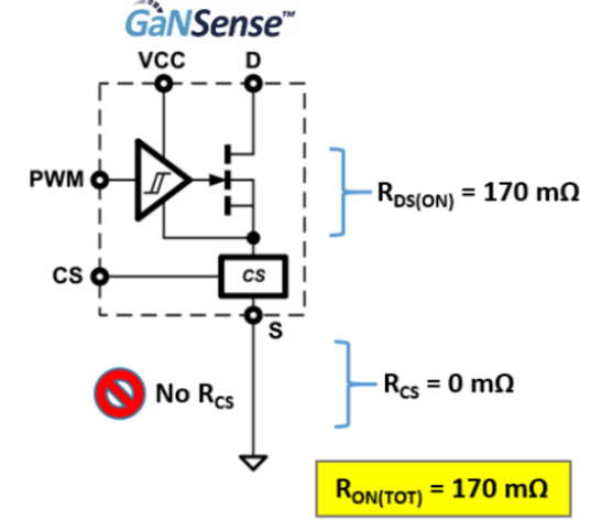
El Segundo, CA based gallium nitride (GaN) power ICs supplier Navitas Semiconductor has announced the launch of its third generation (3G) GaNFast power IC with integrated proprietary GaNSense technology. According to Navitas, GaNSense technology integrates critical, real-time autonomous sensing and protection circuits to further improve reliability and robustness, while increasing energy savings and fast-charging benefits of GaN IC technology (Figure 1).

Speaking of reliability, the company has shipped over 30 million GaNFast power ICs with over 116 billion device hours in the field and zero reported GaN field failures, said Stephen Oliver, vice president of corporate marketing at Navitas Semiconductor. Plus, he added, each GaNFast power IC shipped offers a 4-10x reduced carbon footprint and saves 4 kg of CO2 emission as compared to legacy silicon chips.
In essence, said the maker, GaNSense technology integrates circuits for real-time, accurate and fast sensing of system parameters including current and temperature. Consequently, it enables a patent-pending lossless current-sensing capability, which improves energy savings by up to an additional 10% compared to prior generations, as well as further reduces external component count to shrink system footprint. In addition, to protect both the device and the surrounding system from potentially dangerous system condition, the IC is designed to transition rapidly to a cycle-by-cycle sleep-state. Another key feature includes an autonomous standby-power which automatically reduces standby power consumption when the GaN power IC is in idle-mode, helping to further reduce power consumption.
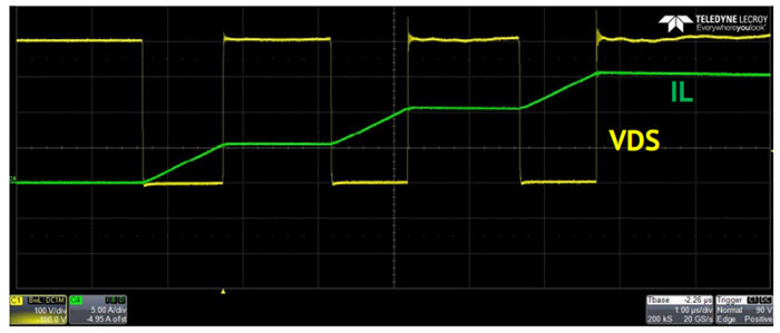
“With the integration of GaNSense circuit, it takes only 30 ns from detection to protection, which is 600% faster than discrete GaN implementation,” stated Oliver. With high current-measurement accuracy and response time, GaNSense technology reduces dangerous over-current spikes by 50% and delivers dependable, glitch-free operation with no ringing for improved system reliability (Figure 2), added Oliver. Furthermore, he continued, the new 3G GaNFast IC is immune to transient voltages up to 800 V and provides tight gate waveform control and voltage regulation.

The new family of 3G GaN power ICs with integrated GaNSense technology offers ten products, all of which include the core GaNFast integration of GaN power, drive, control and protection. All are rated at 650-V/800-V with 2 kV ESD protection, and RDS(on) ranging from 120 mΏ to 450 mΏ in 5×6 and 6×8 mm PQFN packages. The manufacturer said that 3G GaN power ICs are optimized for modern power conversion topologies, including high-frequency quasi-resonant flyback, active-clamp flyback and PFC boost. Per Navitas Semiconductor, these topologies are popular to deliver the fastest, most efficient and smallest chargers and adapters within the mobile and consumer markets.
Target markets include fast-chargers for smartphones and laptops, as well as all-in-one PCs, TVs and home networking and automation. GaN power IC with GaNSense technology has been implemented in Lenovo’s YOGA 65 W laptop charger and Xiaomi’s Note 11 Pro+ smartphone fast chargers with 120 W capability. Both these products are in mass production phase, said Navitas. Meanwhile, Navitas rang the Nasdaq opening bell on 20 October 2021 and started trading on the Nasdaq floor.


