This year, during APEC 2021, the virtual exposition unveiled several high-voltage gallium nitride (GaN) FETs from old and new players in the market. Key amongst them was Power Integrations, a strong believer in silicon. The company displayed an off-Line CV/CC ZVS flyback integrated switcher IC with 750 V PowiGaN FET, active clamp drive and synchronous rectification. Called InnoSwitch4-CZ, it was tailored for 60 W ultra-compact USB PD 3.0 charger for mobile phones and laptop computers.
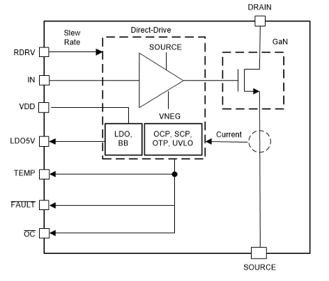
Likewise, Texas Instruments disclosed its first automotive 650 V GaN FET with integrated driver, protection and active power management (Figure 1) [1]. Designated LMG3525R030-Q1, it reduces the size of electric vehicle (EV) onboard chargers by 50% compared to existing silicon or SiC solutions, claims TI. According to applications manager Ramanan Natarajan, “fast switching integrated gate driver enables a 59% reduction in the size of power magnetics in EV chargers. An industrial version includes a 600 V GaN FET.”

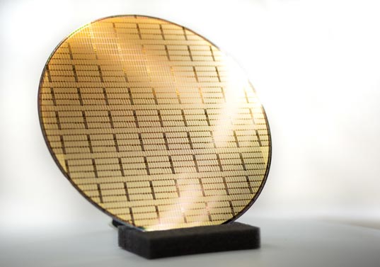
Meanwhile, other suppliers in the race to deliver integrated high-voltage GaN FETs and ICs include Infineon Technologies, GaN Systems, Navitas Semiconductor, and STMicroelectronics amongst others. In partnership and collaboration with Panasonic Corp., Infineon Technologies announced plan to move to 8-inch wafer manufacturing for its second generation (Gen 2) 650 V GaN HEMTs (Figure 2). Like the jointly developed Gen 1 devices, known as Infineon’s CoolGaN and Panasonic’s X-GaN, the second generation will be based on the normally-off GaN-on-Silicon transistor structure. According to the partners, Gen2 will be developed as 650 V GaN HEMT, targeting high- and low-power SMPS applications, renewables, and motor drives. Also, the market launch of the new 650 V GaN Gen2 devices is planned for the first half of 2023.

While GaN power semiconductor supplier GaN Systems inked a semiconductor capacity agreement with auto maker BMW, mobile fast-charger producer Navitas Semiconductor disclosed plans to extend the reach of its integrated high-voltage GaNFast power ICs to higher-power consumer, EV, solar, and data center applications. Additionally, Navitas is also ramping fast GaN charger shipments to the likes of Dell, Lenovo, LG and Xiaomi and more, according to market research company Yole Développement, Lyon, France. Concurrently, the GaN power IC provider announced plans to go public in a special purpose acquisition company. This critical industry development follows in the footsteps of US-based GaN manufacturer, Transphorm, which went public in 2020, noted Yole.
Likewise, STMicroelectronics continues to expand its MasterGaN portfolio with the addition of MasterGaN3 and MasterGaN5 power system packages. MasterGaN5, for instance, integrates a gate driver and two enhancement mode GaN power transistors in half-bridge configuration in a single power package. The integrated power GaNs offer 650 V drain-source blocking voltage and RDS(on) of 450 mΩ, while the high side of the embedded gate driver is supplied by the integrated bootstrap diode. Other MasterGaN5 features include UVLO protection on both the lower and upper driving sections to prevent the power switches from operating in low efficiency or dangerous conditions, and the interlocking function avoids cross-conduction conditions. The extended range of the input pins allows easy interfacing with microcontrollers, DSP units or Hall-effect sensors. It comes in a compact 9×9 mm QFN package and operates in the industrial temperature range of -40 °C to 125 °C.
As more and more suppliers join the race and market adoption rises, the market projection for high-voltage GaN devices and powers ICs looks promising.
Reference
[1] “Virtual APEC 2021 Illuminates Emerging Technologies and Trends” by Ashok Bindra, IEEE Power Electronics Magazine, September 2021, p.55.


