Suzhou, China based gallium nitride on-silicon (GaN-on-Si) startup Innoscience Technology, the producer of high performance, normally-off e-mode GaN-on-Si FETs, has announced the official launch of its international operations in the USA and Europe. The nascent company is now poised to support global customers through the addition of design and sales support facilities in Santa Clara, California, USA and Leuven, Belgium. Currently, in California, there are four staff members involved in technical marketing and design support, with plans to increase that number to eight by the year-end. While Europe is focused on research and development (R&D) and plans to hire an R&D director in the second quarter, according to Denis Marcon, general manager at Innoscience Europe NV (Leuven, Belgium). He added, “Our GaN-on-Si devices have passed quality and reliability tests in excess of JEDEC standards.”
Today, Innoscience employs over 1,400 people, mostly in China, which includes roughly 300 R&D experts, all dedicated to delivering high performance and high reliability GaN power devices that can be widely used in a variety of applications, including cloud computing, electric vehicles (EVs) and automotive, portable devices, mobile phones, chargers and adapters.

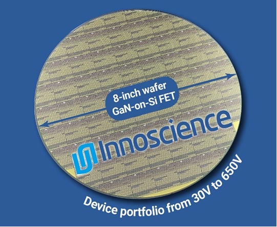
As per the release, the company has a wide portfolio of low voltage (LV) and high voltage (HV) devices, ranging from 30 V to 650 V (Figure 1), and has shipped more than 30 million parts for use in applications including USB PD chargers/adapters, datacenter power supplies, mobile phones and LED drivers. It is also eyeing EV chargers, and for that it is in the process of qualifying its high voltage devices for automotive applications. Meanwhile, the European arm is also planning to develop HV GaN devices (1200 V), and GaN power ICs, in collaboration with Belgium’s R&D hub imec.
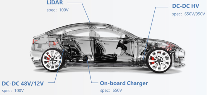
The product roadmap shows e-mode GaN-on-Si LV high-electron-mobility-transistors (HEMTs) in the 30 V to 150 V range, while HV members offer 650 V breakdown capability. In the LV arena, one 40 V member and two 100 V parts are in production, while the manufacturer is sampling 60 V, 100 V and 150 V GaN-on-Si HEMTs with ultra-low on-resistance of 7 mΩ. In addition, the manufacturer is also developing 30 V, 40 V and 100 V parts with RDS(on) of less than 6 mΩ and higher current capability. Also, plans are underway to introduce automotive qualified devices in 2022/2023 (Figure 2), said Marcon. “Innoscience’s fabs are AEC-Q100 certified for automotive parts productions and the company is already working with automotive customers to qualify specific devices,” added Marcon.

Likewise, in the HV area, Innoscience is offering 650 V parts with maximum RDS(on) going from 140 mΩ to 800 mΩ and current handling capability varying from 2 A to 17 A. Packaging options include DFN 8×8, DFN 5×6 and wafer scale. Concurrently, several 650 V members with ultra-low on-resistance and higher current capability with several packing options are under development.
Additionally, the company is also offering several demo boards using both LV and HV GaN HEMTs. Marcon indicated that several commercial products using Innoscience’s GaN technology are in production. For example, a 40 V bidirectional InnoGaN offers overvoltage protection inside a smartphone’s battery management system. “It is the world’s first GaN inside a smartphone,” claims the supplier. Likewise, a commercial 45 W fast charger uses InnoGaN devices to offer a peak efficiency of >95% and 4x higher power density. Likewise, a 120 W PD charger, manufactured by companies like Nubia and Tencent, uses InnoGaN devices to offer 94.5% efficiency with a power density of 2.2 W/cm3 (36 W/inch3). Similarly, InnoGaN devices have been used in the manufacture of server rack power supplies, such as 3000 W ac-dc converter and 300 W dc-dc converter, offering high efficiency and power density in comparison to silicon based solutions.
Founded in December 2015, the Chinese startup claims to be the largest integrated device manufacturer that is fully focused on GaN technology. Presently, it has two wafer fabs, including the world’s largest dedicated 8-inch GaN-on-Si site in Suzhou, China, feata uring the latest, advanced, high-throughput manufacturing equipment. Currently, according to the manufacturer, the Suzhou facility has a capacity of 10,000 8-inch wafers per month, which will be ramped up to 14,000 8-inch wafers per month later this year and 70,000 8-inch wafers per month by 2025.


